
- Mass Spectrometry for Energy Transformation and Astrochemistry
- Extreme Ultraviolet Electronic Structure Characterization and Lithography
- Electronic Structure Characterization for Operando Micro/Nano Devices
- High-sensitive, Space-Resolved and Time-Resolved Electron Spin Dynamics
- In-situ/Operando Soft X-ray Spectroscopy and Scattering
- Soft X-ray Ptychographic Nanoscopy
- Resonant Coherent Scattering
- High Throughput In-situ/Operando Tender X-ray Spectroscopy
- Tender X-ray Spectromicroscopy and Ptychography
- Test Beamline

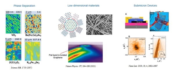
Scientific Scope 1: Reducing the beam spot size to sub-micron and nanoscale levels enables the direct visualization of emergent quantum phenomena. This capability is critical for probing micro-scale phase separation in metal-insulator transitions and iron-based superconductors. Furthermore, it allows for the study of low-dimensional materials, particularly twisted systems like graphene and transition metal dichalcogenides, where nanoscale moiré patterns host novel correlated states. Finally, nanoscale beams are indispensable for resolving the electronic structure within operational sub-micron devices, bridging the gap between macroscopic measurement and nanoscale function.

Scientific Scope 2: The use of soft X-ray photons provides enhanced bulk sensitivity and elemental specificity compared to ultraviolet light. This enables the detection of bulk electronic states and allows researchers to distinguish them from surface states. Furthermore, the technique is well-suited for probing the electronic structure of buried interfaces, such as two-dimensional electron gases (2DEGs). The requirement for surface cleanliness is also less stringent due to the higher penetration depth of soft X-rays. Additionally, this energy range facilitates resonant ARPES experiments, which provide elemental sensitivity by tuning the photon energy to specific absorption edges.
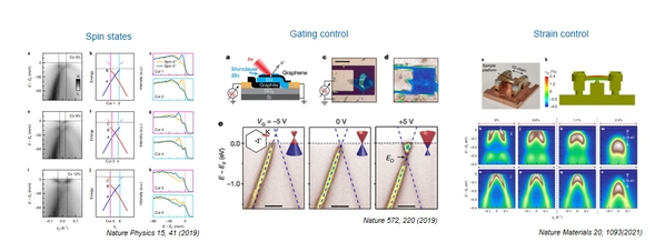
Scientific Scope 3: Advancing micro- and nano-devices requires the ability to control electronic states across multiple degrees of freedom. Our experimental system is designed for this purpose, combining several key techniques: spin-resolved analysis via a VLEED detector, in situ electrical gating to probe functional electronic structure in device-relevant conditions, and the application of uniaxial strain to induce and study novel quantum phases.