


Optics and Instrumentation

1. Beamline Optical System
1.1 Integrated Beamline Optical Design Metrology
A new beamline optical system design method is proposed, in which the calculation of synchrotron radiation source flux distribution, monochromator spectral resolving power, mirror reflectance and grating diffraction efficiency are integrated together to evaluate the whole beamline optical system performance. The key idea is shown in the figure as below.
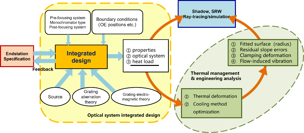
The modules for the optical system integrated design have been used in some HALF and HLS beamline designs. The beamline transmission rate can be optimized while the RP and other design requirements are met.
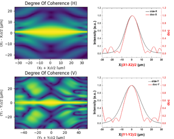
1.2 Beamline Design for Coherent Synchrotron Radiation Source
HALF is a DLSR, which light is coherent or partial coherent. For the coherent beamline, the beamline needs to preserve the coherence; for the incoherent beamline, the effect from the coherent properties needs to be taken care of.
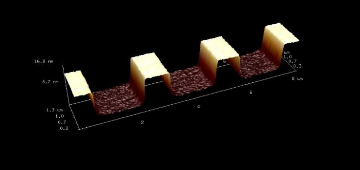
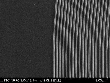
For the coherence preservation, the beamline will use fewer optical elements, simpler surface shape with high requirements on surface error (figure error ~ 1 nm rms). The partial-coherent simulation has also been performed for all beamlines.
Coherent beamline with fewer optical elements and simple surface shape
Partial coherent simulation
For all the beamlines, coherent-related calculation has been performed to make sure that the diffraction effect will not decrease the beamline performance greatly, especially at the exit slit.
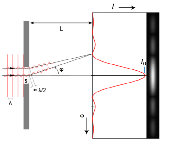
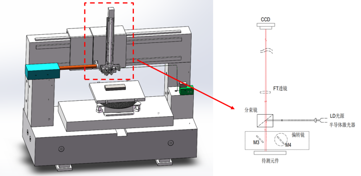
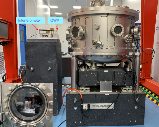
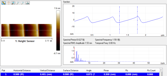
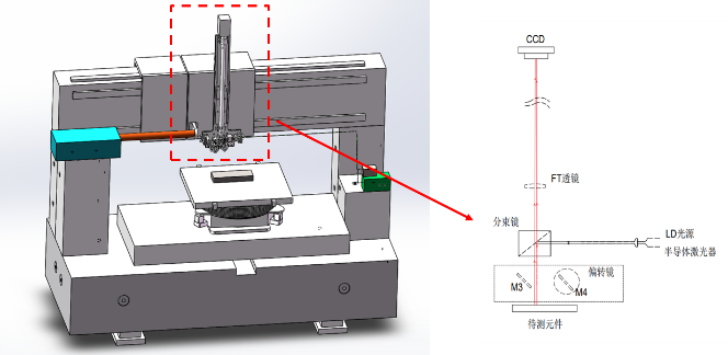
1.3 Interferometric Method for Spectral Resolving Power Test
BL10 can operate in the high-spectral-resolving-power mode. Its spectral resolving power (RP) which can reach 105@400 eV while using grating 2400 l/mm and cff = 10. The typical RP measurement is gas absorption spectra, but it is inaccurate for high RP case. In order to accurately measure the RP, the Mach-Zehnder (M-Z) interferometry is adopted, as shown in the figure below. The longitudinal coherent length L = λ2/Δλ will be measured by this method, and the RP = λ/Δλ can be calculated.
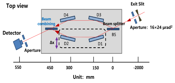
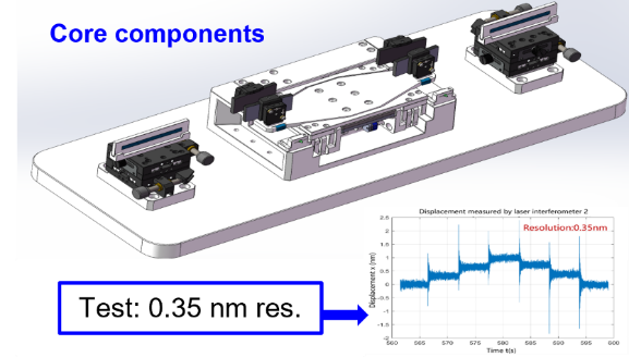
The highest RP measured by M-Z interferometry is determined by the working range of the displacement stage; the working energy (400 eV) determined that the minimum step of the stage is ~ 1 nm. The mechanical components design and test have been finished, as shown in the figure below. The core specifications have been met.
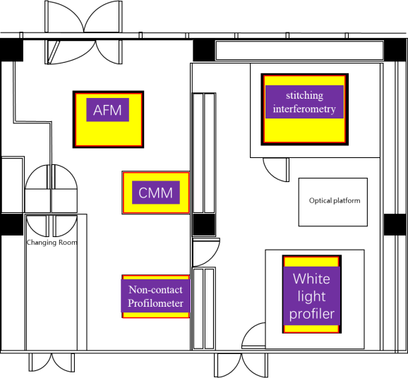
2. Optical Metrology Lab
Optical Metrology Lab (OML) is dedicated to ensuring the optimal performance of beamline optical systems through a comprehensive suite of characterization techniques. Our core mission encompasses the high-precision inspection of key optical components (mirrors, gratings, and substrates), the critical study of mounting-induced and thermal deformations, and R&D in active optical devices. Leveraging dedicated beamlines and state-of-the-art lab-based systems, we conduct fundamental and applied research on X-ray optics and novel metrology methods to support current and future light source facilities.
2.1 Layout of Optical Metrology Lab
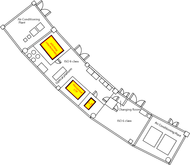
Key Features:
Areas: 130 m2 + 150 m2
Temperature Stability: Maintains stability within 0.05 K.
Vibration: VC-G.
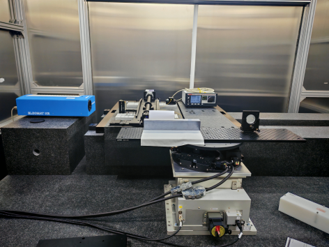
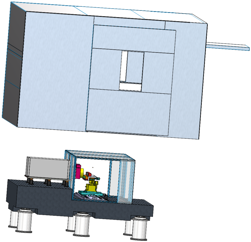
2.2 Slope Measuring Systems (Long Trace Profiler - LTP)
Our laboratory features two customized LTP systems (vertical and horizontal configurations) capable of measuring mirror surfaces in all orientations. These systems offer high-repeatability slope and curvature measurements for X-ray mirror up to 1.5 meters in length.
Key Features:
Repeatability: 30 nrad RMS for both systems.
Angular Range: ±4 mrad.
Temperature Stability: Maintains stability within 0.05 K over 48 hours.
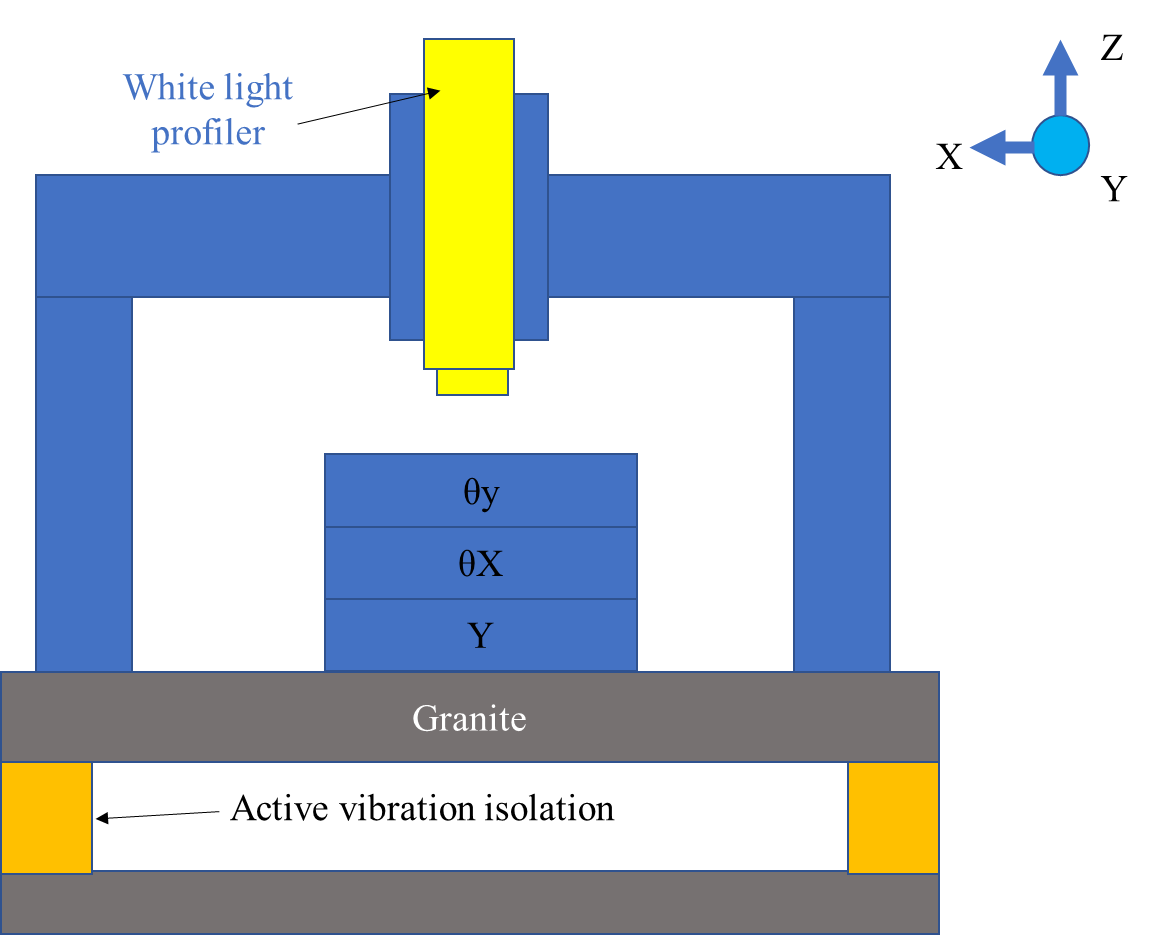
2.3 Mirror Roughness Measurement
We utilize a white light profilometer system for measuring optical micro-roughness over large areas. The system operates on a marble platform with active vibration isolation legs to ensure precision.
Key Features:
Reproducibility: 0.06 nm RMS.
Roughness Measurement Range: Up to 1.2 meters.
Environmental Stability: Active vibration isolation and temperature control.
2.4 Stitching Interferometer
Our 2D surface metrology system employs hybrid stitching algorithms for high-resolution figure measurement. The system is designed for repeatability and stability, with ongoing development towards ultra-high stability.
Key Features:
Reproducibility: 0.18 nm RMS at 0.15 mm (unfiltered data) with hybrid stitching.
Agreement with LTP: 0.19 nm RMS.
Capabilities: Measures 2D surface profiles with high precision and repeatability.
2.5 Members
|
|
|
|
|
Shuai Zhao shuai.zhao@ustc.edu.cn Postdoc | Zhengkun Liu zhkliu@ustc.edu.cn Senior Engineer | Huiyun Wang wanghuiyun@zjgdz.cn Engineer | Xueqin Xu xxq@ustc.edu.cn Engineer | Yifan Zhao zhaoyifan@zjgdz.cn Engineer |
3. Beamline Instruments
3.1 Plane Grating Monochromator (PGM)
Our laboratory has developed an ultra-high spectral resolution plane grating monochromator (PGM) based on a stroke bearing shaft. This independently developed monochromator achieves a spectral resolving power of 100,000 and demonstrates excellent stability, fully meeting the requirements of newer generation beamlines.
Key features:
Resolving power:100, 000
Mechanical resolution of rotation: 50 nrad
Stability:<50nrad RMS
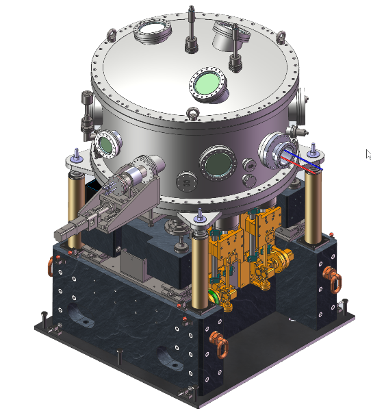
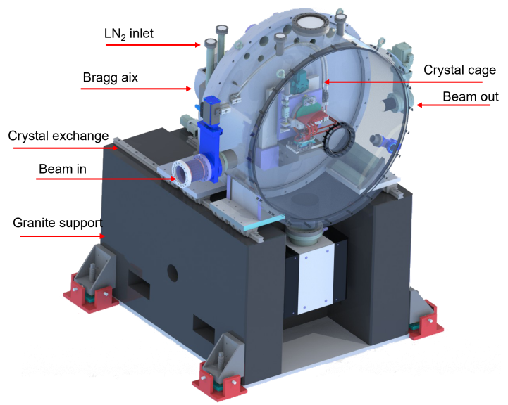
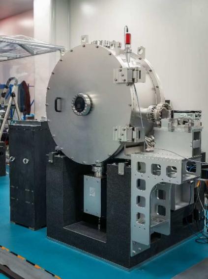
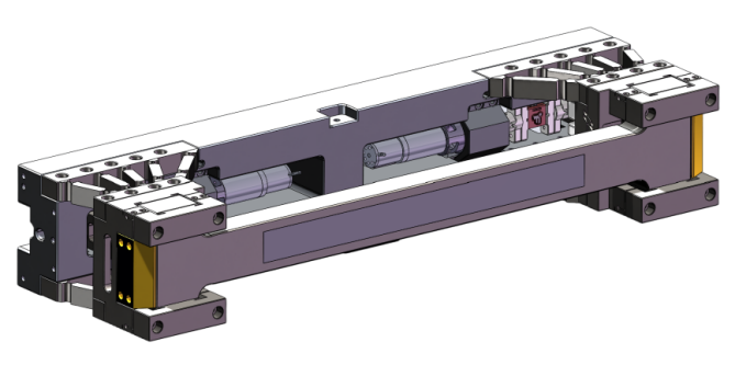
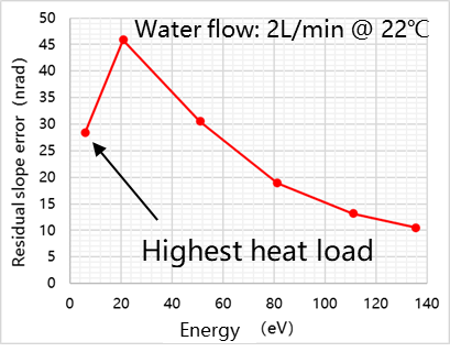
3.2 Double Crystal Monochromator (DCM)
The demand for monochromators with exceptional precision and vibration stability is critical for beamlines at diffraction-limited storage-ring light sources. To address this need, our laboratory has developed a high-stability double-crystal monochromator (DCM) featuring a high-stiffness flexure hinge. Operating with a liquid nitrogen flow rate of 2 L/min, the system achieves a remarkable relative crystal stability of 10 nrad RMS.
Key features:
Cooling scheme: Liquid nitrogen cooling
Energy range:2.3-8 keV
Relative stability in pitch direction:10 nrad RMS with LN2 flow rates 2L/min.
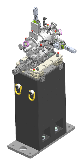
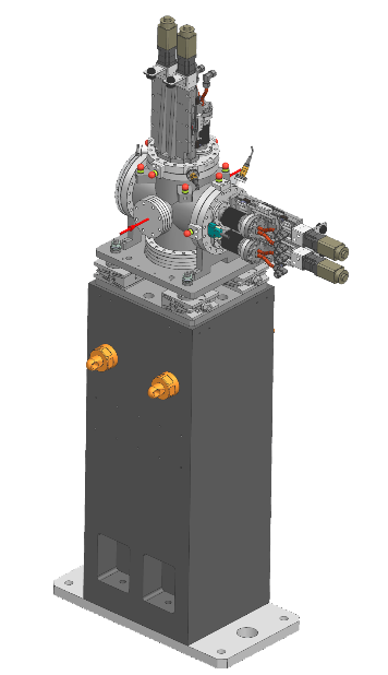
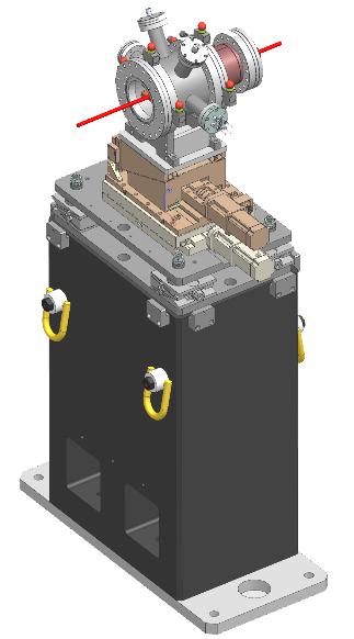
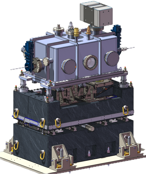
3.3 Mirror systems
The mirror cases accommodates different types of mirrors and provides high-stability support, ultra-high vacuum environment and high-precision adjustment for the mirrors to achieve the transmission, collimation and focusing of x-rays.
3.4 Bendable mirror
The bendable mirror is used to meet the needs of collimating or focusing X-rays to different experimental stations for various scientific requirements. It is necessary to adjust the surface shape dynamically with high repeatability.
3.5 General Units
We have also developed other general-purpose beamline equipments, including precision slits, apertures, and beam position monitors.
Precision slit |
Adjustable Aperture |
PBPM |
3.6 Members
Qiuping Wang qiuping@ustc.edu.cn Professor |
Xuewei Du xwdu@ustc.edu.cn Senior engineer |
Shen Wei weishen@ustc.edu.cn Senior engineer |
Yang Peng kaseva@ustc.edu.cn Engineer |
Zhanglang Xu xulang@ustc.edu.cn Postdoc |
Qi Zhou zhouqi0714@ustc.edu.cn Engineer |
4. Front-Ends and Beamline Vacuum System
4.1 Front-End of Beamlines
The front end of the beamline, as a crucial component connecting the storage ring and the beamline, is an indispensable part of the construction of the Hefei Advanced Light Facility. The front end is used to implement the functions of vacuum protection, personal protection, component protection, beam confining and beam diagnosis.
In phase I, 11 front ends will be installed, including 10 undulator front ends and 1 bending magnet front end. 10 undulator beamlines will be open to users, while the bending magnet will be used for machine study. The undulator front end will receive 17.3 kW/mrad2 of peak power density and 4.7 kW of the total power. These front ends adopt a common modular design, which is based on compatibility with various front ends. The difference lies in the selection of individual components and the variations in parameters.
4.2 Beamline Vacuum System
The beamline vacuum system is responsible for the following tasks:
Formulation of clean vacuum standards
Overall planning of vacuum components such as pumps, valves, and gauges
Development of vacuum differential components
Cleaning of carbon deposits on the surfaces of optical components
4.3 Members
Ming Chen Senior Engineer chenming@zjgdz.cn |
Lijun Tang Engineer tanglijun@zjgdz.cn |
|
5. Beamline Thermal Management
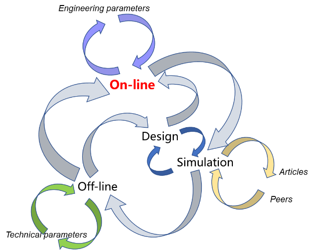
With the rapid advancement of fourth-generation synchrotron radiation sources, beamline optical components with hundred-nanoradian slope error face unprecedented thermal load challenges under extremely high photon flux and coherence conditions. Thermal effects have become one of the key factors limiting the performance of these optical elements. The Beamline Thermal Management Laboratory is dedicated to establishing a closed-loop technical framework integrating design, simulation, and experimental validation to ensure the high-performance operation of critical beamline components. Our mission includes developing high performance cooling strategies for front-end systems, key beamline components, and precision optical elements. We also conduct systematic studies of beamline-related thermal phenomena and develop advanced devices such as thermally controlled adaptive mirrors. Leveraging the dedicated beamline, we investigate the relationships among power, temperature, and deformation, providing essential support for the sustainable development of future synchrotron radiation facilities.
5.1 Optimization Method of Thermal Deformation
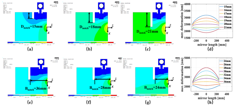
For the 4th generation synchrotron radiation facilities, the heat load of first mirrors and plane mirrors within PGMs had flown to more than hundred watts, while their thermal deformation should less than 100-nanoradian slope error. To rapidly achieve this across their full working energy range to fulfill the requirements of the construction, our laboratory had developed optimized cooling techniques including mitigate edge effects and enhance structural symmetry, based on thermal bending moment balance and high heat transfer coefficient techniques.
![]()
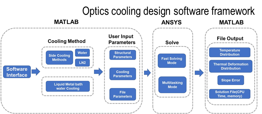
5.2 Optical component cooling scheme automatic optimization software
After the confirmation of the cooling optimization technique, the cooling scheme designs may become a kind of routine work. We had developed a software based on the heat load power density, optics dimension and target thermal deformation via the ANSYS and matlab, who can calculate and optimize the cooling type and dimension automatically. Further down the line, our lab will cooperate with beamline optics lab to design the beamline integrated design software.
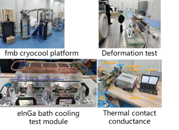
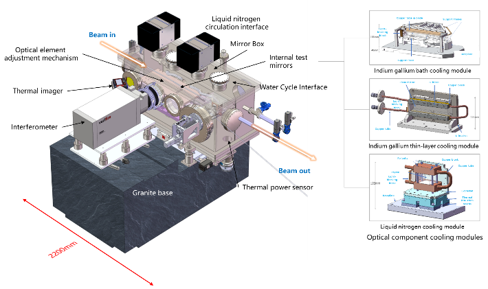
5.3 Thermal Management Test Platform for Offline and Online
To systematically investigate and resolve "thermal" issues associated with the beamline, a comprehensive understanding of the dynamic changes in factors influencing the opto-mechanical system is imperative. These factors primarily encompass thermal deformation, system thermal stability, and thermally induced mirror distortion. To address the core, our lab set up the off-line devices and on-line end station. The off-line devices can help us iterate our researches rapidly, while the on-line end station can do them systematically.
5.4 Members
Jie Chen Senior Engineer jiechen9@ustc.edu.cn |
Dezhi Diao Engineer diaodezhi@zjgdz.cn |
Qiuzi Yu Engineer yyqqzz@ustc.edu.cn |
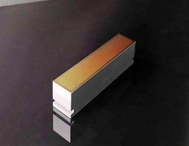
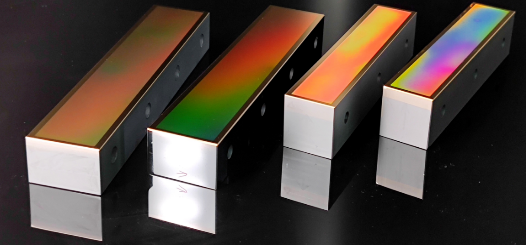
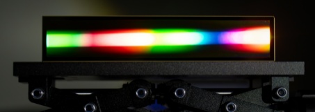
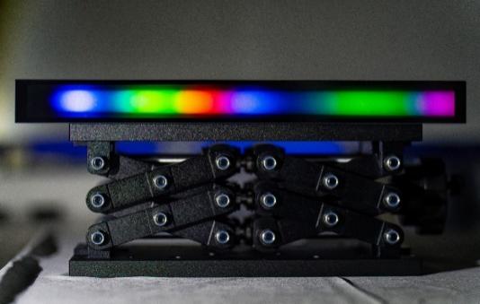
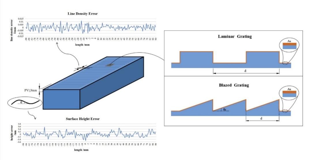
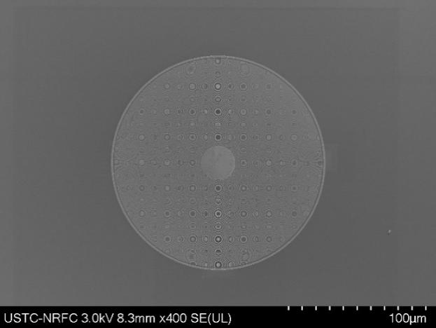
6. Fabrication of X-ray Diffraction Grating
Our primary mission is to fabricate high-end soft X-ray – EUV gratings, e.g., with low substrate figure error and line density distribution, and small blazed angles.
Laminar and blazed gratings, featuring no ghost lines and low stray lights, can be fabricated by using holographic lithography and ion beam etching/chemical etching.
Variable line spacing gratings with high precision line density distribution have been realized with a deformable mirror, eliminating the error of line density distribution formed in the traditional holographic gratings.
Recently, more than 10 diffraction gratings have been developed for domestic synchrotron sources, including a free electron laser source.
6.1 Synchrotron Radiation Gratings and Capabilities
Method | Holographic lithography+ ion beam etching /chemical etching |
Substrate | Plane/curved |
Size (length) mm | Up to 400mm |
Grating center line density (lines/mm) | 50-3600 |
Grating surface error | Better than 100nrad |
Figure error (PV / RMS) nm | Better than 4/1 |
Grating profile | Laminar/ blazed(blazed angle≥0.4°) |
Groove roughness (rms) | Better than 0.4nm |
Coating | Au, Pt, Ir, Cr, etc. |
Residual error of line density Δn/n (@ 2400 lines/mm) | 2e-6 |
6.2 Measurement of grating parameters
* A long trace profiler for the measurement of the line density coefficient and slope error of gratings,
* A scanning stitching interferometer for the measurement of the height error of gratings,
* The Metrology Beamline at the Hefei Light Source for the characterization of the efficiency and stray light of the fabricated gratings @ 5-1000eV.
6.3 Members
Liu Zhengkun zhkliu@ustc.edu.cn Senior Engineer |
Qiu Keqiang blueleaf@ustc.edu.cn Ass. Professor |
Liu Ying liuychch@ustc.edu.cn Ass. Professor |
Hong Yiling ylhong@ustc.edu.cn Professor |
Fang Mingyin myfang@ustc.edu.cn Engineer |
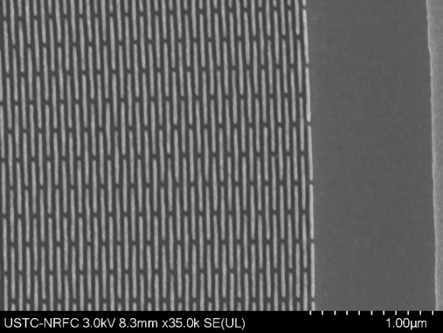
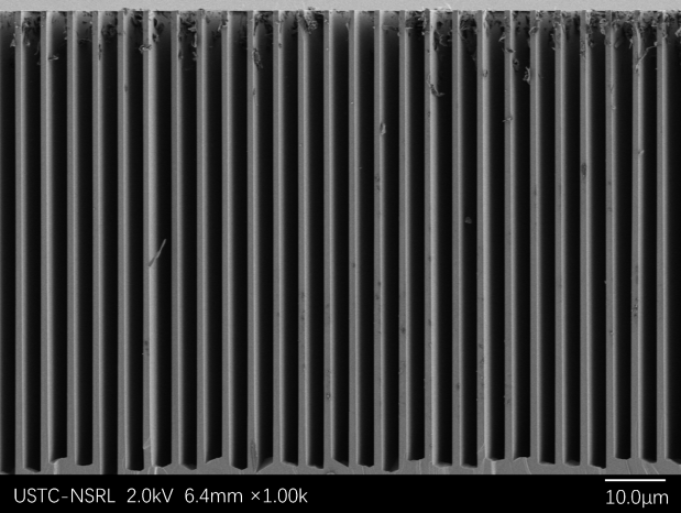
7. Fabrication of Micro-Nano Optics
The Micro-Nano Optics Group is dedicated to the advancement of micro and nano optics for X-ray, neutron and Extreme Ultraviolet (EUV) applications. We focus on three key areas: optical component design, advanced fabrication technologies, and precision metrology. The primary objective is to support the operational and performance enhancement needs of major light source facilities, including HLS and HALF beamlines, by providing custom-designed, high-performance optics and pioneering new techniques. Furthermore, we are committed to transitioning these capabilities into reliable commercial solutions for the broader scientific and industrial communities.
7.1 Key Optical Components
7.1.1 X-ray Optics: Zone Plates and Imaging Gratings
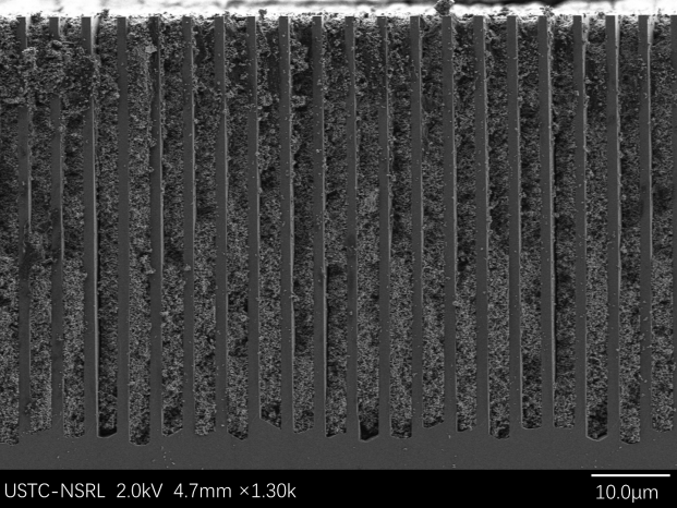
Zone Plates: We specialize in fabricating high-resolution Fresnel zone plates for focusing X-rays. Development projects are focused on achieving an outermost zone width of 15 nm for ultra-fine probes, while zone plates for illumination applications are designed to produce customizable spot sizes in the 10-60 μm range. These optics are designed and optimized for specific beamlines and techniques, such as nano-spectroscopy and coherent diffraction imaging.
Imaging Gratings: Phase and absorption gratings are developed for advanced interferometric imaging and wavefront sensing. Processes are established that enable the fabrication of gratings with minimum periods down to 4 μm, which are crucial for quantitative phase-contrast imaging and wavefront correction techniques.
7.1.2 EUV Optics: XIL Transmission Gratings and Zone Plates
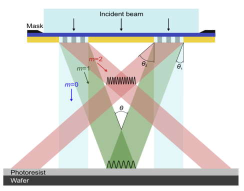
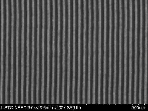
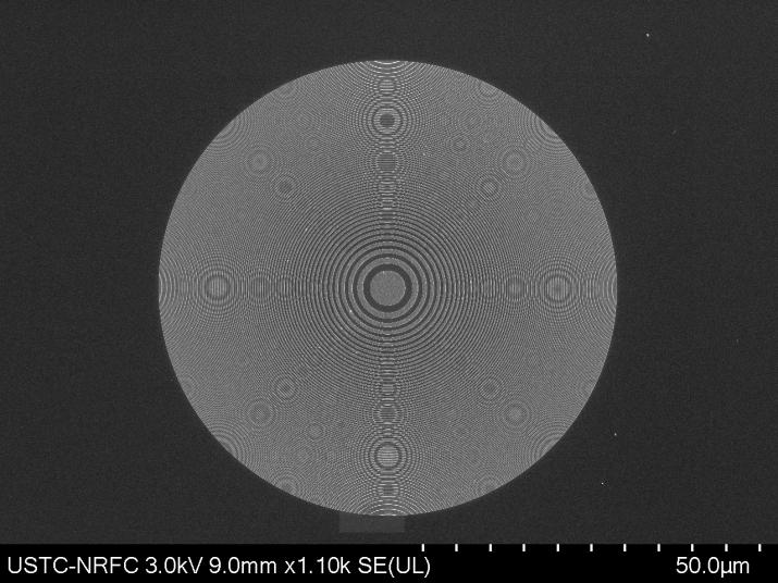
For the EUV spectral range, we fabricate transmission optics including zone plates and gratings. A key focus is the development of high-efficiency transmission gratings with periods down to 20 nm, supporting applications in EUV interference lithography, mask detection, high-resolution spectroscopy, and focusing.
7.1.3 In-Situ Chip Devices (Gas-Solid / Liquid-Solid / Liquid-Liquid)
Specialized microfluidic chips are designed and fabricated to enable real-time studies of dynamic processes under controlled environments. These chips are engineered to withstand challenging conditions, including vacuum and variable temperatures or electromagnetic field, thereby facilitating research in catalysis, battery materials, and interfacial science by providing controlled sample environments (gas-solid, liquid-solid, liquid-liquid).
7.2 Capabilities & Supporting Facilities:
The fabrication and characterization capabilities are supported by extensive in-house facilities and collaborations, enabling a diverse array of projects to be handled.
7.2.1 Nanofabrication Facilities
A comprehensive micro-nano fabrication platform has been established, enabling a complete process chain that includes lithography, thin-film deposition, dry etching, wet etching, and electroplating. This platform is compatible with wafer sizes up to 8 inches. A variety of materials and substrates are utilized:
Substrates: Silicon nitride membranes, silicon wafers, and other custom materials can be accommodated upon request.
Patterned Materials: Organic resists, Au, Ni, as well as other materials for thin layers.
Feature Size and Scale: Features ranging from below 50 nm to several microns are reliably produced.
Aspect Ratios: A practical rule of thumb for achievable structure thickness is up to 10 times the smallest feature size.
7.2.2 Characterization and Metrology
The quality and performance of optics are ensured through comprehensive characterization using:
Scanning Electron Microscopy (SEM) for high-resolution imaging of nanostructures.
Atomic Force Microscopy (AFM) for precise topographical measurement.
Probe Profiler for surface shape analysis.
Custom Optical/EUV Test Stations for direct performance validation under application-like conditions.
7.3 Looking Forward
The development roadmap is aligned with the evolving needs of next-generation light sources. Key goals include the deployment of optics with 15 nm resolution by 2030, the advancement of EUV grating technology, and the expansion of the suite of in-situ chips. Discussions are welcomed to collaborate on specific project requirements and to develop the optics needed to power advanced scientific research.
Contact us to discuss how your research can be supported.
7.4 Members